Semiconductor Process Engineer Resume Guide
Semiconductor process engineers are responsible for overseeing the development, testing, and production of semiconductors. They design processes to ensure quality control in manufacturing from start to finish, analyze data generated during product tests, and troubleshoot any problems that arise.
You have the technical know-how to make a semiconductor manufacturer’s production run smoothly. But hiring managers aren’t aware of your qualifications yet, so you must write an impressive resume that catches their eye.
This guide will walk you through the entire process of creating a top-notch resume. We first show you a complete example and then break down what each resume section should look like.
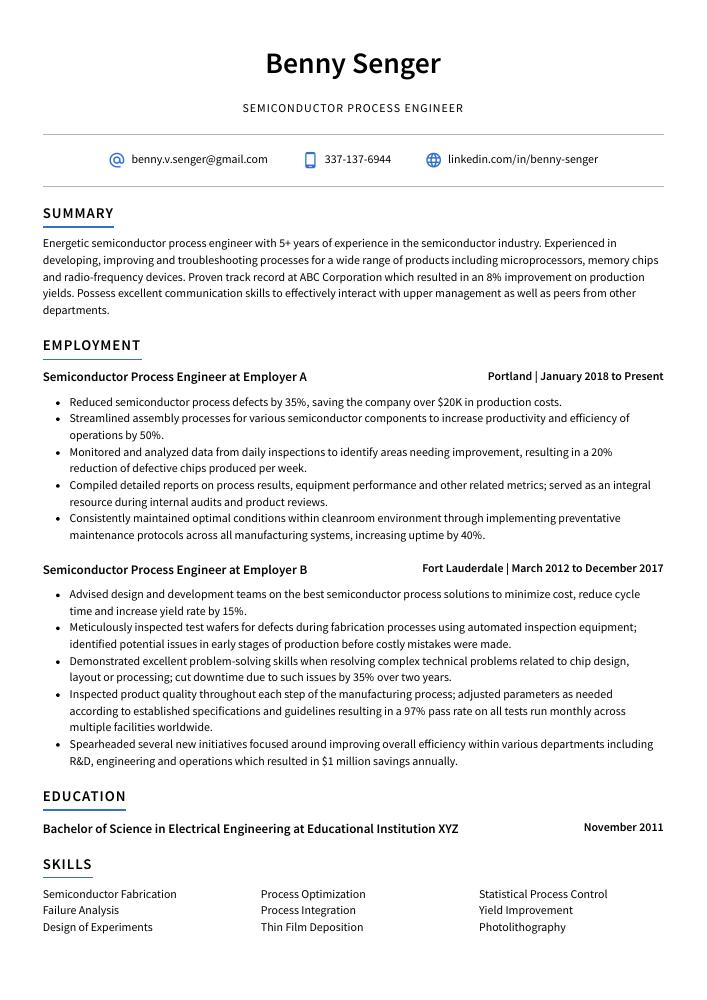
Table of Contents
The guide is divided into sections for your convenience. You can read it from beginning to end or use the table of contents below to jump to a specific part.
Semiconductor Process Engineer Resume Sample
Benny Senger
Semiconductor Process Engineer
[email protected]
337-137-6944
linkedin.com/in/benny-senger
Summary
Energetic semiconductor process engineer with 5+ years of experience in the semiconductor industry. Experienced in developing, improving and troubleshooting processes for a wide range of products including microprocessors, memory chips and radio-frequency devices. Proven track record at ABC Corporation which resulted in an 8% improvement on production yields. Possess excellent communication skills to effectively interact with upper management as well as peers from other departments.
Experience
Semiconductor Process Engineer, Employer A
Portland, Jan 2018 – Present
- Reduced semiconductor process defects by 35%, saving the company over $20K in production costs.
- Streamlined assembly processes for various semiconductor components to increase productivity and efficiency of operations by 50%.
- Monitored and analyzed data from daily inspections to identify areas needing improvement, resulting in a 20% reduction of defective chips produced per week.
- Compiled detailed reports on process results, equipment performance and other related metrics; served as an integral resource during internal audits and product reviews.
- Consistently maintained optimal conditions within cleanroom environment through implementing preventative maintenance protocols across all manufacturing systems, increasing uptime by 40%.
Semiconductor Process Engineer, Employer B
Fort Lauderdale, Mar 2012 – Dec 2017
- Advised design and development teams on the best semiconductor process solutions to minimize cost, reduce cycle time and increase yield rate by 15%.
- Meticulously inspected test wafers for defects during fabrication processes using automated inspection equipment; identified potential issues in early stages of production before costly mistakes were made.
- Demonstrated excellent problem-solving skills when resolving complex technical problems related to chip design, layout or processing; cut downtime due to such issues by 35% over two years.
- Inspected product quality throughout each step of the manufacturing process; adjusted parameters as needed according to established specifications and guidelines resulting in a 97% pass rate on all tests run monthly across multiple facilities worldwide.
- Spearheaded several new initiatives focused around improving overall efficiency within various departments including R&D, engineering and operations which resulted in $1 million savings annually.
Skills
- Semiconductor Fabrication
- Process Optimization
- Statistical Process Control
- Failure Analysis
- Process Integration
- Yield Improvement
- Design of Experiments
- Thin Film Deposition
- Photolithography
Education
Bachelor of Science in Electrical Engineering
Educational Institution XYZ
Nov 2011
Certifications
Certified Semiconductor Manufacturing Professional
Semiconductor Equipment and Materials
May 2017
1. Summary / Objective
Your resume summary should be a concise overview of your qualifications and experience as a semiconductor process engineer. Highlight key accomplishments such as the successful implementation of new processes, cost savings initiatives, or any awards you may have received for excellence in engineering. Additionally, mention any certifications or specializations that make you stand out from other candidates.
Below are some resume summary examples:
Professional semiconductor process engineer with 5+ years of experience in semiconductor device fabrication and characterization. Skilled in developing processes for various applications including CMOS, DRAM, and optoelectronic devices. Expertise includes statistical analysis, defect reduction strategies, particle control methods and wafer-level testing. At XYZ Corporation oversaw the yield improvement project that resulted in a 50% increase in overall product quality.
Determined semiconductor process engineer with 10+ years of experience in the semiconductor industry. Skilled in developing new processes and improving existing ones to meet customer requirements while maintaining high quality standards. At XYZ, led development of a novel lithography patterning process that improved yields by 40%. Experienced at troubleshooting complex problems and optimizing production efficiency through data-driven methodology.
Committed semiconductor process engineer with 8+ years of experience in semiconductor wafer fabrication and design. Demonstrated success leading projects from concept to completion, troubleshooting complex manufacturing problems, and optimizing processes for cost reduction and efficiency gains. Looking to bring expertise in advanced lithography techniques and innovative problem-solving skills to ABC Tech’s team of world-class engineers.
Amicable and detail-oriented semiconductor process engineer with 5+ years of experience in the industry. Seeking to apply strong problem-solving and communication skills to join ABC Tech’s team as a Process Engineer, helping develop cutting edge technologies that shape our future. Previous accomplishments include designing an advanced chip fabrication process which resulted in 20% yield improvement and cost savings up to $100K/year.
Dependable and results-oriented semiconductor process engineer with 5+ years of experience in the design, development and implementation of integrated circuit fabrication processes. Experienced in optimizing processes for yield and cost savings using cutting edge technologies such as lithography, plasma etching, deposition and oxidation. At XYZ company executed 10 back end projects resulting in improved defect density by 40%.
Diligent semiconductor process engineer with 6+ years of industry experience in R&D and production. Experienced in developing, optimizing, and validating semiconductor processes for various applications. Seeking to join ABC Tech as a senior process engineer to use my expertise towards improving the yield rate by 15%. Key achievements include reducing the defect rate by 25% while boosting throughput efficiency by 30%.
Talented semiconductor process engineer with 5+ years of experience designing, developing and optimizing wafer fabrication processes. Experienced in semiconductor IC design and testing, as well as working closely with the production team to ensure high-quality products. Seeking a position at ABC Technologies to utilize skills in problem solving, data analysis and technical writing for innovative product development.
Enthusiastic semi-conductor process engineer with 5+ years of experience in development and design of semiconductor masks for ICs. Possesses an extensive background in lithography, etching, deposition processes, device characterization methods and tools. Aiming to leverage my knowledge to become the next Process Engineer at ABC Tech where I can contribute to cutting-edge chip designs.
2. Experience / Employment
In the experience section, you should provide details on your employment history. This section should be written in reverse chronological order, meaning the most recent role is listed first.
When writing about what you did in each job, stick to bullet points as much as possible; this makes it easier for readers to digest the information quickly. You want to make sure that you give enough detail so that they understand exactly what tasks and results were achieved while working at a certain position.
For example, instead of saying “Developed semiconductor processes,” you could say “Created new process flows for semiconductors using advanced software tools such as Cadence Virtuoso and Synopsys IC Compiler II which resulted in an increase of yield by 20%.”
To write effective bullet points, begin with a strong verb or adverb. Industry specific verbs to use are:
- Designed
- Optimized
- Fabricated
- Analyzed
- Monitored
- Programmed
- Calibrated
- Troubleshot
- Implemented
- Validated
- Inspected
- Documented
- Resolved
- Commissioned
Other general verbs you can use are:
- Achieved
- Advised
- Assessed
- Compiled
- Coordinated
- Demonstrated
- Developed
- Expedited
- Facilitated
- Formulated
- Improved
- Introduced
- Mentored
- Participated
- Prepared
- Presented
- Reduced
- Reorganized
- Represented
- Revised
- Spearheaded
- Streamlined
- Structured
- Utilized
Below are some example bullet points:
- Diligently monitored, controlled and optimized semiconductor fabrication processes to achieve a 5% reduction in defect rate.
- Documented process control procedures and provided technical support for over 30 production runs; improved product yield by 10%.
- Validated new technologies and increased process throughput by 20% through detailed analysis of equipment performance data.
- Analyzed defects using microscopy techniques, identified root cause issues, derived solutions & implemented corrective actions resulting in a 15% improvement in overall quality assurance results.
- Achieved successful transfer of advanced packaging technology from R&D to manufacturing with zero errors or delays within budget parameters specified by management team.
- Structured and implemented semiconductor fabrication processes to manufacture high-volume products, resulting in a 10% increase in production efficiency.
- Introduced new methods for process development and improvement, reducing costs by $20K within 3 months of implementation.
- Optimized existing manufacturing operations through careful analysis of data trends; improved cycle time performance by 25%.
- Assessed the quality and yield outputs from existing processes while providing guidance on corrective actions as necessary; achieved 99% defect free rate across all products produced annually.
- Efficiently managed multiple projects simultaneously with tight timelines and delivered results ahead of schedule; completed over 150+ engineering tasks within 6 months period without sacrificing quality or safety standards.
- Substantially improved process reliability and product yield by 25% through the implementation of cutting-edge semiconductor manufacturing technology.
- Mentored team of 5 junior engineers on advanced Semiconductor Process Engineering principles and technologies, resulting in a 50% improvement in production output within 4 months.
- Facilitated cross-functional collaborations with other engineering teams to optimize processes for new products; accelerated development timeframes by 30%.
- Presented up-to-date technical trends at monthly meetings, keeping management informed about industry advancements; earned praise from senior leadership for knowledge sharing initiatives across the company’s global offices.
- Designed reliable measurement systems to monitor key performance indicators such as temperature control, wafer defect levels and cycle time consistency; minimized machine downtime due to system failure issues by 70%.
- Programmed and operated semiconductor process equipment, resulting in the successful completion of over 20 product development projects with a 45% reduction in production costs.
- Commissioned and maintained multiple pieces of high-tech process engineering equipment; implemented new procedures to reduce downtime by 35%.
- Prepared detailed reports on fabrication yields and machine performance to assess progress toward design goals; identified areas for improvement that resulted in an increase of 7% efficiency gains across all processes.
- Represented the Process Engineering team at client meetings and trade shows, demonstrating extensive knowledge about current developments within the industry as well as technological capabilities available through our company’s products/services.
- Proficiently utilized Computer Aided Design (CAD) software to create accurate three-dimensional models for semiconductor device components & systems prior to actual manufacture/fabrication stage – reducing design cycle time by 25%.
- Fabricated/processed over 500 wafers per month using advanced semiconductor process engineering techniques, resulting in a 10% production increase.
- Developed and implemented innovative processes to enhance the quality of silicon products; reduced time for product testing by 20%.
- Resourcefully identified and solved critical issues with existing designs and produced cost-effective solutions that improved overall efficiency by 30%.
- Utilized statistical methods such as DOE (Design of Experiments) to analyze data from multiple experiments related to design changes/improvements on semiconductors, validating results through rigorous experimentation protocols.
- Expedited delivery timelines for prototype designs without compromising accuracy or quality; completed projects ahead of schedule resulting in an additional $40K in revenue last quarter.
- Resolved complex reports in semiconductor process engineering for over 20 production lines, eliminating defects by 80% and increasing product yield by 25%.
- Implemented new technologies to improve existing processes that reduced cycle times by 15%, resulting in a $50K annual cost savings.
- Revised tooling design drawings to increase efficiency while maintaining strict safety protocols; decreased changeover time from 8 hours to 4 hours with no quality issues reported.
- Formulated strategic plans for the introduction of new products into existing production operations, which helped boost sales revenue by 10% during the first quarter of operation after launch.
- Competently managed high-volume wafer fabrication activities across three shifts, meeting all targets on schedule within budget constraints and ensuring customer satisfaction levels remained above 90%.
- Coordinated the design, development and implementation of advanced semiconductor processes across 10+ fabrication lines; improved process efficiency by 15% and reduced production time by 40 hours per month.
- Actively monitored process temperature changes and material composition to ensure that all products met quality standards and customer specifications; identified potential issues before they affected the product yield rate.
- Calibrated automated equipment used in multiple stages of the fabrication line, including scrubbers, furnace systems & wafer handlers, resulting in a 20% decrease in downtime due to malfunctions or breakdowns.
- Troubleshot complex problems arising from unexpected chemical reactions during chip manufacturing processes; implemented new control measures which decreased defect rates by 30%.
- Reorganized existing workflows for 3 major assembly lines at different facilities based on cost-benefit analysis models developed using statistical data sources; increased overall profitability by $12 million annually.
3. Skills
Even though two organizations are hiring for the same role, the skillset they want an ideal candidate to possess could differ significantly. For instance, one may be on the lookout for an individual with experience in semiconductor fabrication processes, while the other may be looking for someone with expertise in process integration.
It is essential to tailor your skills section according to each job you are applying for; this will help ensure that it passes through any applicant tracking systems used by employers. You should also make sure to elaborate on the most important skillset listed here throughout other sections of your resume, such as the summary or work experience areas.
Below is a list of common skills & terms:
- Design of Experiments
- Failure Analysis
- Photolithography
- Process Integration
- Process Optimization
- Semiconductor Fabrication
- Statistical Process Control
- Thin Film Deposition
- Wafer Fabrication and Testing
- Yield Improvement
4. Education
Adding an education section to your resume will depend on the level of experience you have. If you are just starting out and don’t have much work experience, mention your education below your resume objective. However, if you already have a few years of relevant semiconductor process engineering under your belt, including an education section might not be necessary at all.
If you do include an education section in your resume for this role, try to highlight courses or topics related to semiconductor process engineering that could show potential employers how well-equipped you are for the job.
Bachelor of Science in Electrical Engineering
Educational Institution XYZ
Nov 2011
5. Certifications
Certifications are a great way to demonstrate your knowledge and proficiency in a particular field. They can help you stand out from other applicants and show potential employers that you are committed to professional development.
When applying for jobs, make sure to include any certifications relevant to the position on your resume. This will give hiring managers an indication of what skills and qualifications you possess that could be beneficial for the role they are trying to fill.
Certified Semiconductor Manufacturing Professional
Semiconductor Equipment and Materials
May 2017
6. Contact Info
Your name should be the first thing a reader sees when viewing your resume, so ensure its positioning is prominent. Your phone number should be written in the most commonly used format in your country/city/state, and your email address should be professional.
You can also choose to include a link to your LinkedIn profile, personal website, or other online platforms relevant to your industry.
Finally, name your resume file appropriately to help hiring managers; for Benny Senger, this would be Benny-Senger-resume.pdf or Benny-Senger-resume.docx.
7. Cover Letter
Cover letters are an important part of the job application process. They are usually made up of 2 to 4 paragraphs and provide a more detailed introduction than your resume alone can. A well-written cover letter allows you to showcase your personality, explain why you’re suitable for the role and demonstrate that you have done some research about the company or organization.
Even though not every job requires one, submitting a thoughtful cover letter is highly recommended as it gives recruiters an insight into who you are beyond what’s written on paper. It also helps create a lasting impression which could be beneficial when competing against other candidates with similar qualifications and experience.
Below is an example cover letter:
Dear Mary,
I am interested in the position of Semiconductor Process Engineer at [company name] and would like to submit my resume for your review. As a process engineer with 6+ years of experience in the semiconductor industry, I have gained extensive knowledge of wafer fabrication processes and equipment. In my current role, I am responsible for developing new processes and improving existing ones to increase yield and productivity.
Through my work, I have developed strong problem-solving skills that have come in handy when troubleshooting process issues. My analytical nature allows me to quickly identify root causes and develop solutions that prevent problems from recurring. I also have a keen eye for detail, which is essential for ensuring adherence to process specifications.
In addition to my technical skills, I am an excellent communicator who is able to effectively collaborate with team members across departments. My ability to build relationships has been crucial in obtaining buy-in from stakeholders on proposed changes or improvements.
I believe that as a Semiconductor Process Engineer at [company name], I could put my skills and experience to good use while making significant contributions towards the success of your organization. Thank you for your time and consideration; I look forward to speaking with you soon about this opportunity.
Sincerely,
Benny
Semiconductor Process Engineer Resume Templates
 Saola
Saola Quokka
 Dugong
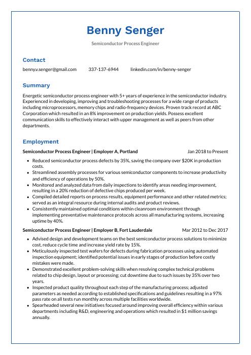 Markhor
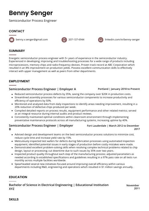 Fossa
Fossa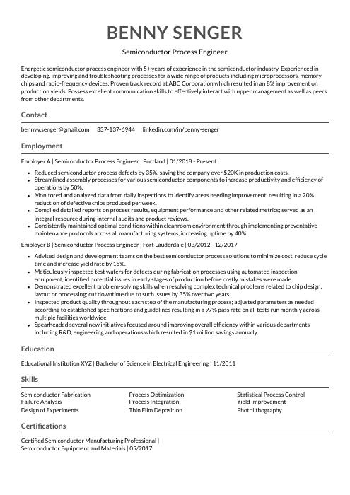 Indri
Indri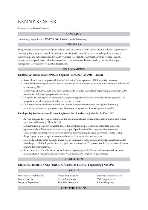 Numbat
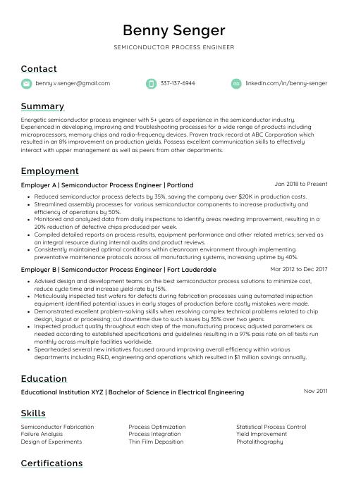 Lorikeet
 Cormorant
 Echidna
 Kinkajou
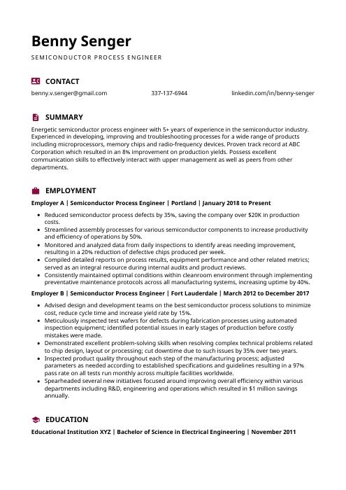 Hoopoe
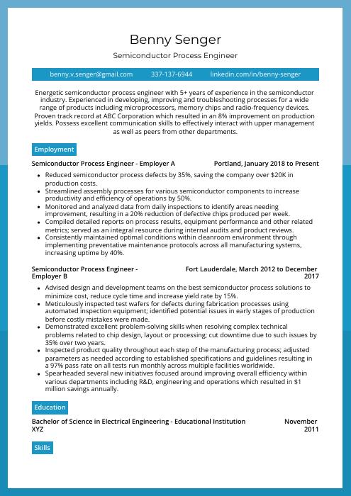 Rhea
Rhea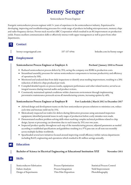 Gharial
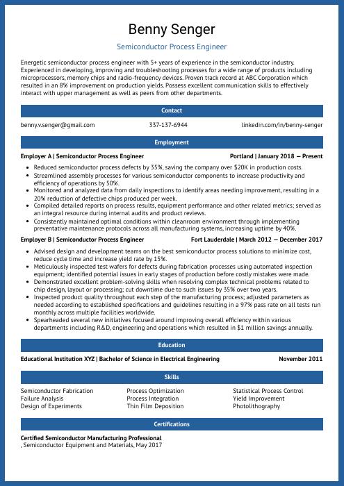 Ocelot
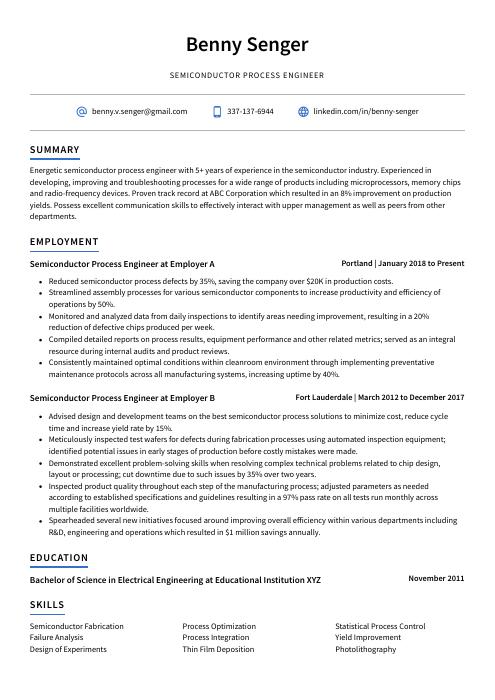 Axolotl
 Pika
Pika Bonobo
 Jerboa